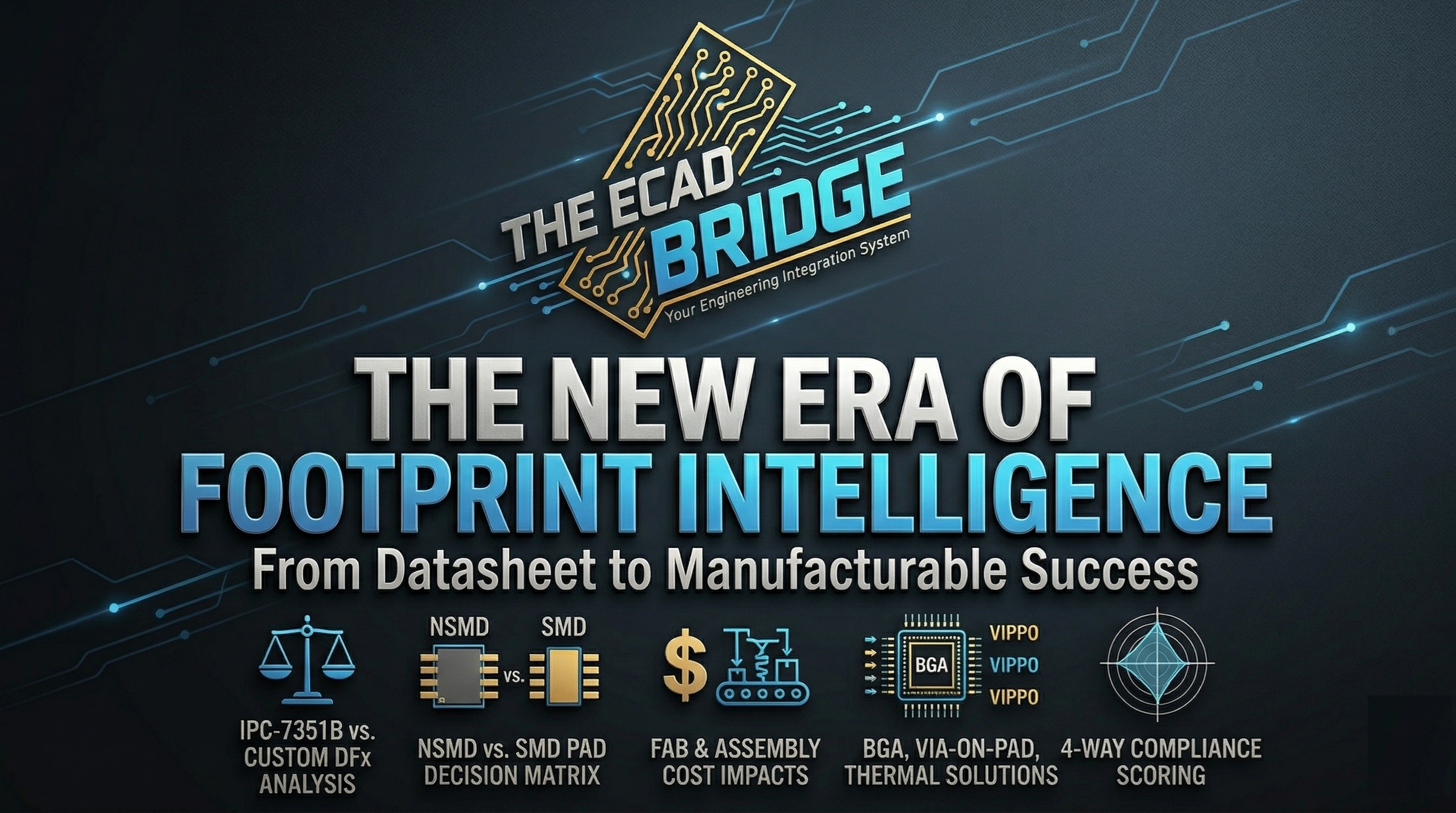
In the high-stakes world of hardware engineering, a footprint is never "just a land pattern." It is the critical interface where electrical theory meets manufacturing reality. For a Hardware Development Engineer or an ECAD Librarian, choosing the right footprint variant whether it’s a standard IPC-7351B pattern or a specialized Custom DFx configuration can be the difference between a smooth product launch and a costly manufacturing nightmare.
But how do we move beyond "standard" libraries to make truly informed decisions?
The answer lies in the Footprint Analyzer, a tool built to decode the DNA of component datasheets and weigh them against the world's most rigorous manufacturing standards.
The Dilemma: IPC-7351B vs. Custom DFx
Every design begins with a choice: Density Level A, B, or C?.
While IPC-7351B provides a fantastic mathematical baseline for solder fillets defining Toe, Heel, and Side goals for standard packages it is …
Unlock Full Article
Log in with your Google account to read the complete article and join the ECAD Bridge community.
Continue with Google
— Article from E-Cad Bridge —