Let's be honest.
Most PCB engineers are using a ₹50 lakh EDA tool like a glorified drawing board.
You route traces. You run DRC. You export Gerbers. You fill in a checklist manually. You email it to the fab and hope nothing slips through.
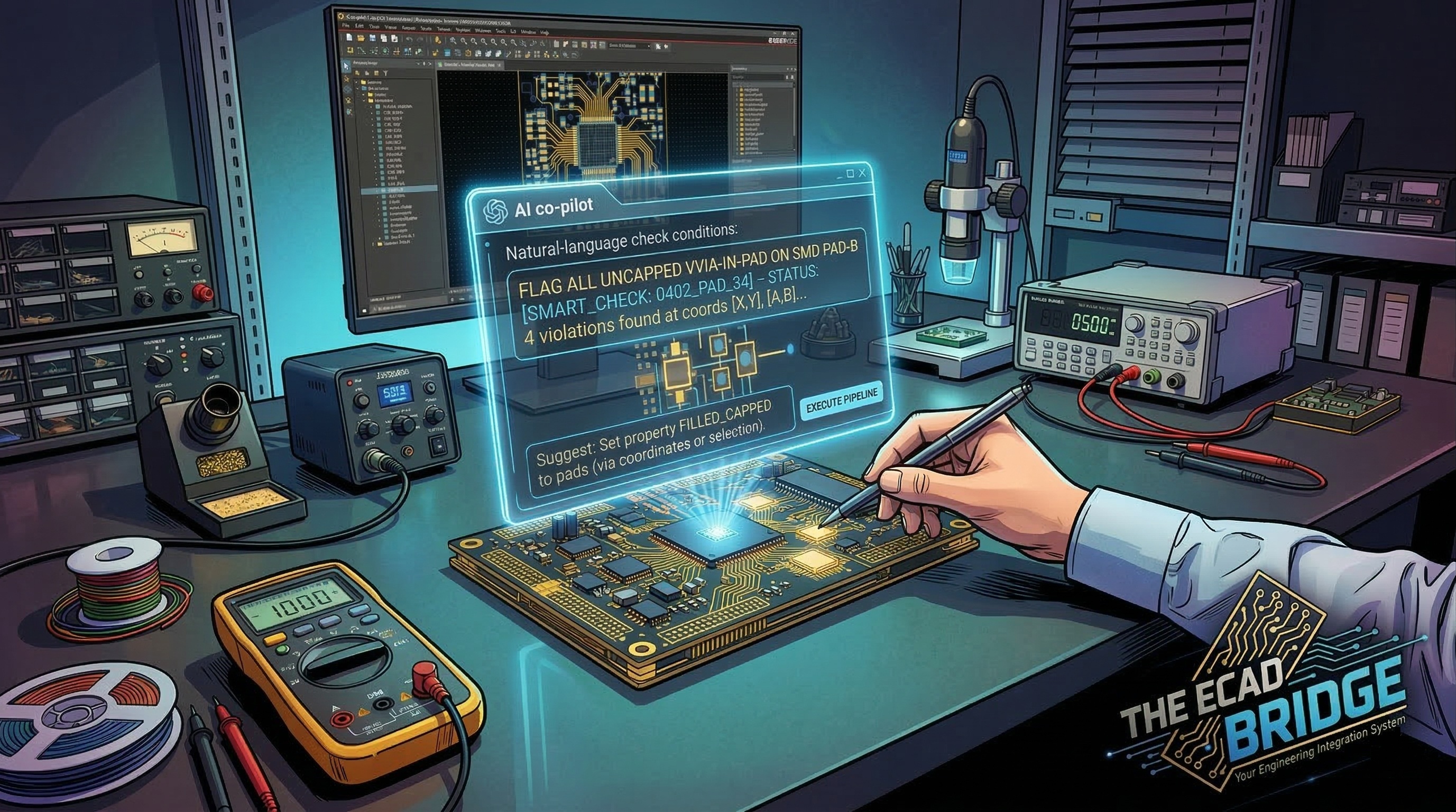
Meanwhile, that same tool is sitting on a complete, queryable database of every net, every via, every dielectric constant, every impedance constraint in your design — and you're not asking it anything.
That's not an EDA problem. That's a workflow problem. And AI is about to make it embarrassingly visible.
🤖 The Co-Pilot Shift Nobody Is Talking About
Everyone in electronics is debating whether AI will replace PCB designers.
Wrong question.
The real shift is quieter and more immediate: AI is becoming the layer between your design intent …
Unlock Full Article
Log in with your Google account to read the complete article and join the ECAD Bridge community.
Continue with Google
— Article from E-Cad Bridge —