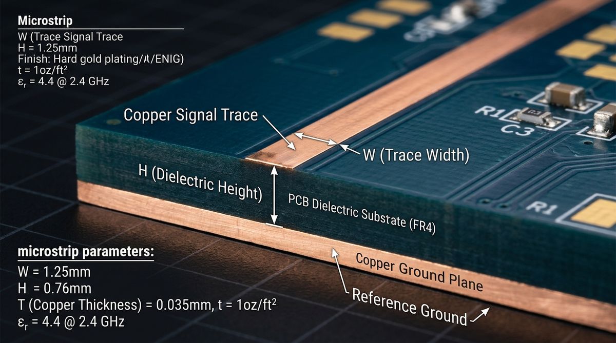
Microstrip Impedance
RF / Transmission Line • IPC-2141
info REFERENCE: IPC-2141 Formula
Zo = (87 / √(εr + 1.41)) × ln(5.98H / (0.8W + T))
High-fidelity engineering formulas for RF transmission lines, embedded hardware, and IPC-standard PCB fabrication with real-time parametric computation.
RF / Transmission Line • IPC-2141
Zo = (87 / √(εr + 1.41)) × ln(5.98H / (0.8W + T))
dBm ↔ Watts ↔ Vrms
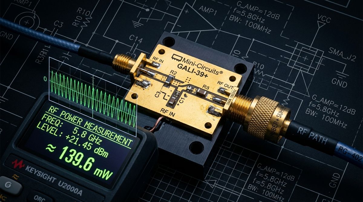
P(mW) = 10^(dBm/10), Vrms = √(P_watts × Z)
RF / High-Freq Conductor
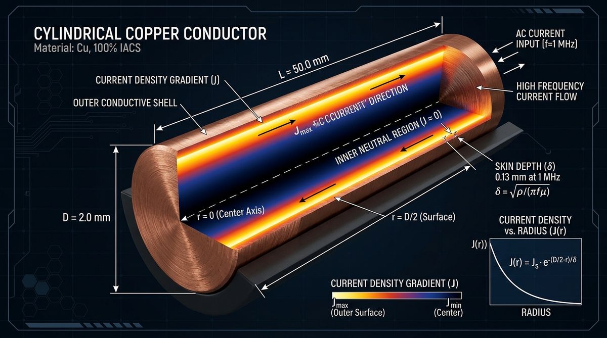
δ = 1 / √(π · f · μ · σ)
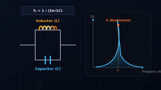
RF / Filter Design
f₀ = 1 / (2π · √(L · C))
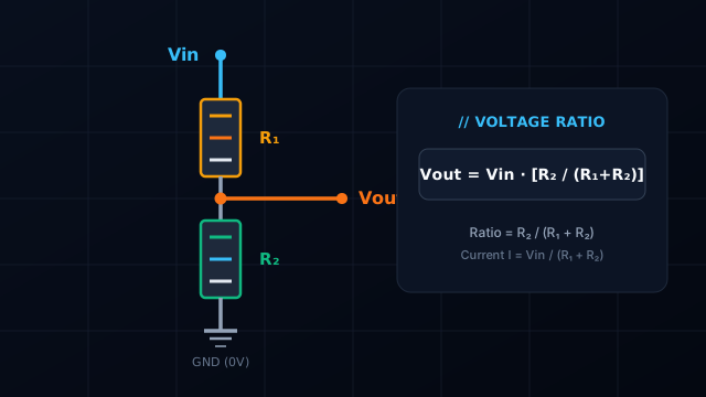
Embedded / Analog Design
Vout = Vin × (R2 / (R1 + R2))
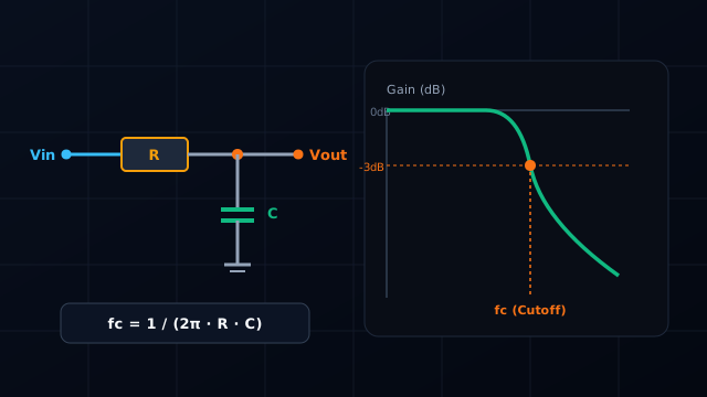
Low-Pass / Time Constant
fc = 1 / (2π · R · C), τ = R · C
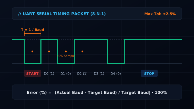
Embedded / MCU Clock
BRR = Round(fCLK / (Over × Baud)), Max allowed error: ±2.5%
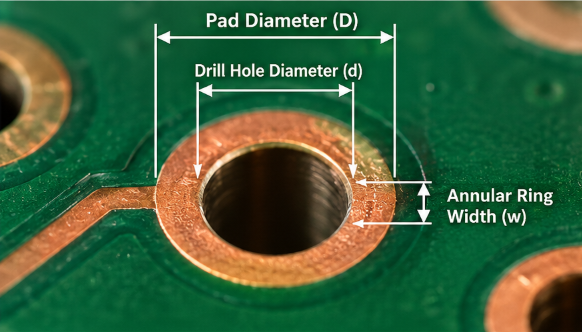
PCB / LIBRARY DESIGN
Ring = (Pad - Hole) / 2. Class 2 requires ≥ 0.05mm internal, ≥ 0.125mm external.
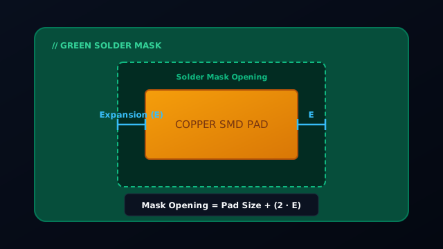
LIBRARY / FOOTPRINT DESIGN
Mask = Pad + (2 × Expansion). Solder dam = Pitch - Mask.
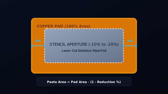
STENCIL / QFN (IPC-7525)
Window panes prevent solder voiding under large thermal pads. Standard coverage: 50% - 70%.
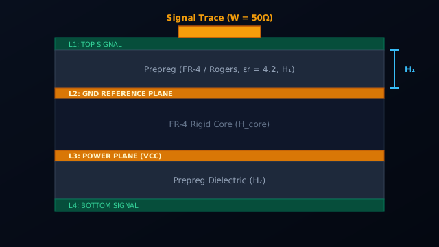
SIGNAL INTEGRITY / LAYER STACK
Zdiff ≈ 2 × Zo × (1 - 0.48 × e^(-0.96 × s/h))
STACKUP / WARPAGE OPTIMIZATION
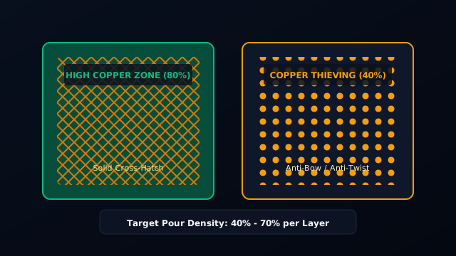
Symmetric copper distribution prevents thermal warpage during reflow soldering.
FABRICATION / IPC-600K
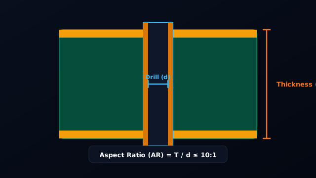
AR = Board Thickness / Drill Diameter. AR ≤ 8:1 is standard low-cost fabrication.
PCB CURRENT CAPACITY
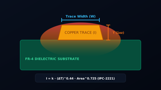
Area = (I / (k · ΔT^0.44))^(1 / 0.725), where k = 0.048 external, 0.024 internal.
PCB / VIA THERMAL RATING
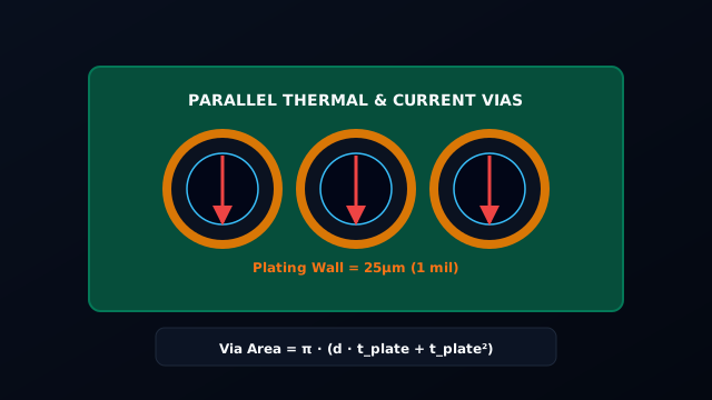
Cross-sectional area of hollow copper cylinder: Area = π × (D · t - t²).
PCB POWER INTEGRITY
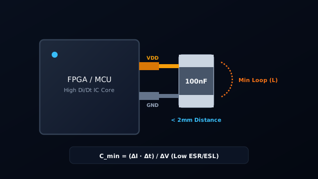
Cmin = ΔI · Δt / ΔV. Place 100nF ceramic capacitor adjacent to each IC power pin.
High-frequency single-ended microstrip impedance calculation adhering to the IPC-2141 standard specification. Simulates characteristic impedance (Z₀), propagation delay (tpd), and geometric aspect ratio.